当今硬件
It is important to understand commodity hardware because specialized hardware is in retreat(消退).
Scaling these days is most often achieved horizontally instead of vertically, meaning today it is more cost-effective to use many smaller, connected commodity computers instead of a few really large and exceptionally fast (and expensive) systems.
This is the case because fast and inexpensive network hardware is widely available.
There are still situations where the large specialized systems have their place and these systems still provide a business opportunity(机会), but the overall(总体) market is dwarfed(相形见绌) by the commodity hardware market.
Red Hat, as of 2007, expects that for future products, the “standard building blocks” for most data centers will be a computer with up to four sockets, each filled with a quad core CPU(4核) that, in the case of Intel CPUs, will be hyper-threaded(超线程).
This means the standard system in the data center will have up to 64 virtual processors.
Bigger machines will be supported, but the quad socket, quad CPU core case is currently thought to be the sweet spot and most optimizations are targeted for such machines.
Large differences exist in the structure of computers built of commodity parts.
That said, we will cover more than 90% of such hardware by concentrating on the most important differences.
Note that these technical details tend to change rapidly(技术日新月异), so the reader is advised to take the date of this writing into account.
南桥与北桥的设计
Over the years personal computers and smaller servers standardized on a chipset(芯片组) with two parts:
the Northbridge and Southbridge.
Figure 2.1 shows this structure.
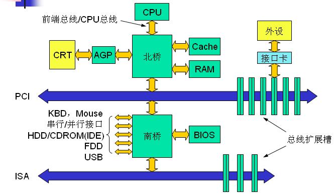
All CPUs (two in the previous example, but there can be more) are connected via a common bus (the Front Side Bus, FSB) to the Northbridge.
The Northbridge contains, among other things, the memory controller, and its implementation determines(决定) the type of RAM chips used for the computer.
Different types of RAM, such as DRAM, Rambus, and SDRAM, require different memory controllers.
To reach all other system devices, the Northbridge must communicate with the Southbridge.
The Southbridge, often referred to as the I/O bridge, handles communicaion with devices through a variety of different buses.
Today the PCI, PCI Express, SATA, and USB buses are of most importance, but PATA, IEEE 1394, serial, and parallel ports are also supported by the Southbridge.
Older systems had AGP slots which were attached to the Northbridge.
This was done for performance reasons related to insufficiently(不够) fast connections between the Northbridge and Southbridge.
However, today the PCI-E slots are all connected to the Southbridge.
Such a system structure has a number of noteworthy consequences(值得注意的结果):
-
All data communication from one CPU to another must travel over the same bus used to communicate with the Northbridge.
-
All communication with RAM must pass through the Northbridge.
-
The RAM has only a single port.
-
Communication between a CPU and a device attached to the Southbridge is routed through the Northbridge.
A couple of bottlenecks are immediately apparent in this design.
需要访问 RAM
One such bottleneck involves(涉及) access to RAM for devices.
In the earliest days of the PC, all communication with devices on either bridge had to pass through the CPU, negatively impacting(负面影响) overall system performance.
DMA 的改进
To work around this problem some devices became capable of direct memory access (DMA).
DMA allows devices, with the help of the Northbridge, to store and receive data in RAM directly without the intervention(介入) of the CPU (and its inherent performance cost).
Today all high-performance devices attached to any of the buses can utilize(利用) DMA.
DMA 带来的问题
While this greatly reduces the workload on the CPU, it also creates contention(争夺) for the bandwidth of the Northbridge as DMA requests compete with RAM access from the CPUs.
This problem, therefore, must be taken into account(不容忽视).
北桥与 RMA 之间的瓶颈
A second bottleneck involves the bus from the Northbridge to the RAM.
The exact details of the bus depend on the memory types deployed.
On older systems there is only one bus to all the RAM chips(芯片), so parallel access is not possible.
Recent RAM types require two separate buses (or channels as they are called for DDR2, see page 8) which doubles the available bandwidth.
The Northbridge interleaves(交错) memory access across the channels.
More recent memory technologies (FB-DRAM, for instance) add more channels.
With limited bandwidth available, it is important for performance to schedule memory access in ways that minimize delays.
As we will see, processors are much faster and must wait to access memory, despite(尽管) the use of CPU caches.
If multiple hyper-threads, cores, or processors access memory at the same time, the wait times for memory access are even longer.
This is also true for DMA operations.
There is more to accessing memory than concurrency, however.
Access patterns themselves also greatly influence the performance of the memory subsystem, especially with multiple memory channels.
In section 2.2 we wil cover more details of RAM access patterns.
北桥的设计
On some more expensive systems, the Northbridge does not actually contain the memory controller.
Instead the Northbridge can be connected to a number of external memory controllers (in the following example, four of them).

优点
The advantage of this architecture is that more than one memory bus exists and therefore total available bandwidth increases.
This design also supports more memory.
Concurrent memory access patterns reduce delays by simultaneously(同时) accessing different memory banks.
This is especially true when multiple processors are directly connected to the Northbridge, as in Figure 2.2.
限制
For such a design, the primary limitation is the internal bandwidth of the Northbridge, which is phenomenal(可察觉的,非凡的) for this architecture (from Intel).
Using multiple external memory controllers is not the only way to increase memory bandwidth.
其他增加 MC 的方式
One other increasingly popular way is to integrate memory controllers into the CPUs and attach memory to each CPU.
This architecture is made popular by SMP systems based on AMD’s Opteron processor.
Figure 2.3 shows such a system.

优点
Intel will have support for the Common System Interface (CSI) starting with the Nehalem processors;
this is basically the same approach:
an integrated memory controller with the possibility of local memory for each processor.
With an architecture like this there are as many memory banks available as there are processors.
On a quad-CPU machine the memory bandwidth is quadrupled without the need for a complicated Northbridge with enormous(巨大的) bandwidth.
Having a memory controller integrated into the CPU has some additional advantages;
we will not dig deeper into this technology here.
缺点
There are disadvantages to this architecture, too.
First of all, because the machine still has to make all the memory of the system accessible to all processors, the memory is not uniform anymore (hence the name NUMA - Non-Uniform Memory Architecture - for such an architecture).
Local memory (memory attached to a processor) can be accessed with the usual speed.
The situation is different when memory attached to another processor is accessed.
In this case the interconnects(互联) between the processors have to be used.
To access memory attached to CPU2 from CPU1 requires communication across one interconnect.
When the same CPU accesses memory attached to CPU4 two interconnects have to be crossed.
NUMA factors
Each such communication has an associated cost.
We talk about “NUMA factors” when we describe the extra time needed to access remote memory.
The example architecture in Figure 2.3 has two levels for each CPU:
immediately adjacent CPUs and one CPU which is two interconnects away.
With more complicated machines the number of levels can grow significantly.
There are also machine architectures (for instance IBM’s x445 and SGI’s Altix series) where there is more than one type of connection.
CPUs are organized into nodes; within a node the time to access the memory might be uniform or have only small NUMA factors.
The connection between nodes can be very expensive, though, and the NUMA factor can be quite high.
Commodity NUMA machines exist today and will likely play an even greater role in the future.
It is expected that, from late 2008 on, every SMP machine will use NUMA.
The costs associated with NUMA make it important to recognize when a program is running on a NUMA machine.
In section 5 we will discuss more machine architectures and some technologies the Linux kernel provides for these programs.
Beyond the technical details described in the remainder(剩余) of this section, there are several additional factors which influence the performance of RAM.
其他影响因素
They are not controllable by software, which is why they are not covered in this section.
The interested reader can learn about some of these factors in section 2.1.
They are really only needed to get a more complete picture of RAM technology and possibly to make better decisions when purchasing(购买) computers.
The following two sections discuss hardware details at the gate level and the access protocol between the memory controller and the DRAM chips.
Programmers will likely find this information enlightening since these details explain why RAM access works the way it does.
It is optional knowledge, though, and the reader anxious to get to topics with more immediate relevance for everyday life can jump ahead to section 2.2.5.